Beijing, Feb. 28 (xinhua) -- graphene research group, advanced carbon materials research department, shenyang institute of materials science, Chinese academy of sciences, has come out with the latest research results.
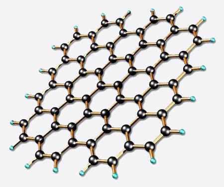
Grain boundary is a common defect in large area graphene films prepared by chemical vapor deposition (CVD). An in-depth understanding of the effects of grain boundaries on the electrical and thermal properties of graphene is important for the development of graphene-based electronics, optoelectronics and thermoelectric devices.
"Although there are many studies on the effect of single grain boundary on the properties of graphene, the effect of grain size on the electrical and thermal properties of graphene on the macro scale is still unclear. The main reason is that CVD growth method based on traditional precipitation (nickel matrix) or surface adsorption growth (copper matrix) mechanism cannot regulate the grain size of graphene in a wide range, and it is particularly difficult to prepare small grain graphene with grain size smaller than the average free path of electrons and phonons (about 1 micron).
Graphene research team using moderate dissolved carbon metal foil as growth substrate, develop a based on the principle of "precipitation - surface adsorption growth" CVD method, only by changing the precipitation temperature was realized the control of the graphene nucleation density, grain size can be produced in ~ 200 nm to ~ 1 micron range adjustable uniform and the quality of the grain boundary perfect fitting single polycrystalline ink film.
On this basis, the research group also obtained the influence of grain size on the electrical conductivity and thermal conductivity of polycrystalline ink-ene, as well as the grain boundary resistivity (~ 0.3kw · m) and grain boundary thermal conductivity (~3.8 109-wm-2k-1).
According to the influence law research group, when the grain size of graphene is reduced from 1 mm to 5 nm, the attenuation range of its thermal conductivity can be up to 300 times, while the attenuation of electrical conductivity is only about 10 times, and the change rate of thermal conductivity and electrical conductivity with the change of grain size is higher than that of typical semiconductor thermoelectric materials. These results can provide useful guidance for controlling the electrical and thermal properties of graphene through grain size engineering and realizing its applications in the fields of electronics, photoelectricity and thermoelectricity.